 HDD magnetic track · MFM mode
AtomExplorer
Compact Multi-Mode AFM
A benchtop AFM built for teaching, QA, and entry-level research. A dual-range scanner (100 μm + 30 μm) switches with one click across 7 imaging modes, and the fully automated workflow takes new users from power-on to first image in 15 minutes.
A Benchtop AFM Designed for Teaching, QA & Entry Research
AtomExplorer distills the core capability of a research-grade AFM into a desktop instrument: a dual-range scanner (100 μm wide-area + 30 μm high-resolution), 7 imaging modes in one tool, and a one-click automated workflow so that new users are fully productive within 15 minutes.
Ideal for undergraduate labs, graduate onboarding, corporate QA checks, and third-party test services — offering the most cost-effective multi-mode AFM in its class.
Dual-Range Scanner
100 μm wide-area + 30 μm high-resolution, one-click switch, no tip change.
7 Imaging Modes
Contact / Tapping / Phase / EFM / KPFM / MFM / PFM all in one box.
Teaching-Friendly
Bilingual GUI (EN/CN), video tutorials, and standard lab kits — undergrads operate independently.
One-Click Automation
Auto laser find-peak / auto approach / auto scan — first image in under 15 minutes.
Specifications & Technology
| Wide-Area XY | 100 × 100 μm |
| High-Resolution XY | 30 × 30 μm |
| Z Range | 10 μm |
| Z Noise Floor | 0.04 nm |
| Scan Angle | 0 – 360° |
| Pixel Resolution | 32×32 – 2048×2048 |
| Max Sample Size | 4″ / 100 mm |
| Max Thickness | 15 mm |
| Motorized XY Stage | Optional 25 × 25 mm |
| Topography | Contact / Tapping / Phase |
| Electrical | EFM / KPFM (lift mode) |
| Magnetic | MFM (lift mode) |
| Piezoelectric | PFM (contact) |
| Architecture | FPGA digital |
| Feedback Loop | up to 50 kHz |
| Lock-in Amp | 1 built-in, >500 kHz BW |
| Sync Channels | Up to 8 synchronous |
| Control Software | AtomControl Lite (EN/CN) |
| Analysis Suite | Roughness / Section / Particles / 3D |
| Dimensions | 420 × 380 × 520 mm |
| Weight | ~ 35 kg |
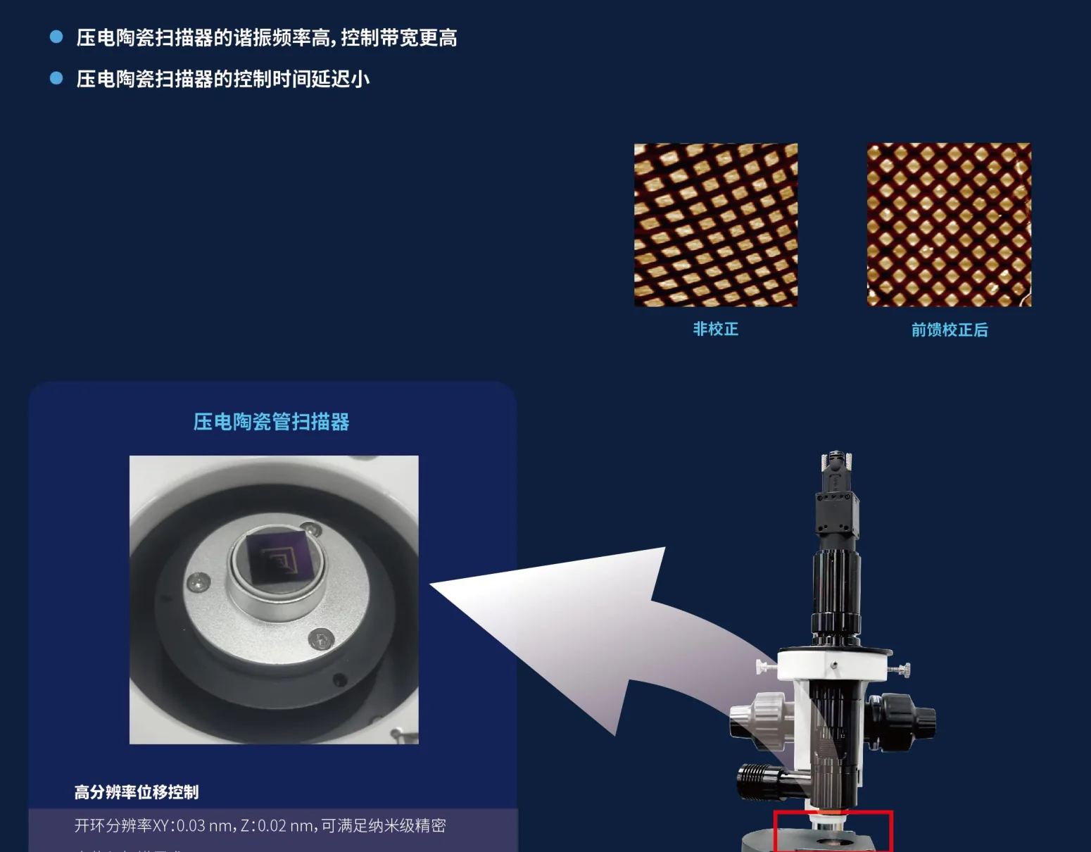
Dual-Range Scanner
A 100 μm wide-area loop and a 30 μm high-resolution loop share one scan head — switch in software, no hardware swap. A single instrument covers the two typical AFM teaching tasks: "see the big picture" and "see the fine detail".
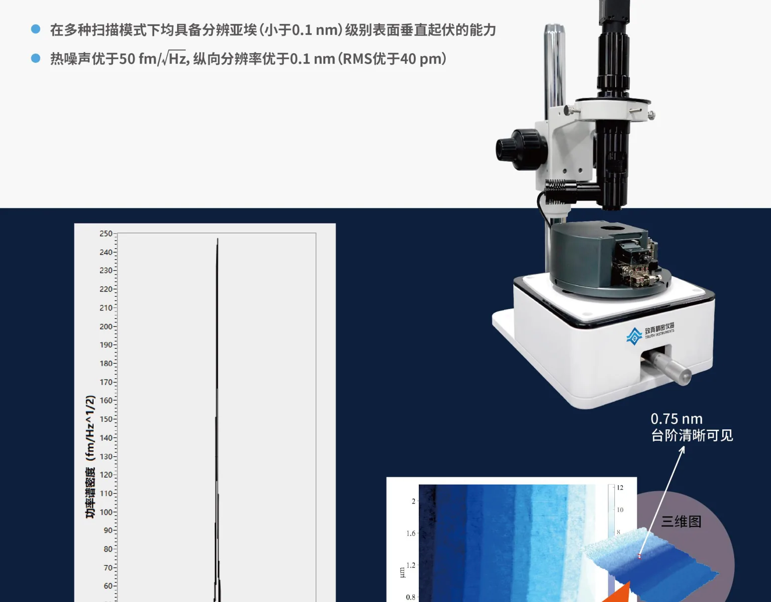
In the high-resolution range, Z noise drops to 0.04 nm — enough to resolve a graphene single-layer step or a self-assembled monolayer thickness.
7 Modes in One Box
Contact / Tapping / Phase topography + EFM / KPFM electrical + MFM magnetic + PFM piezoelectric — an entry-level instrument covers every common AFM topic up through graduate-level coursework. No upgrade path required.
Compared with same-price instruments that only support topography + tapping, AtomExplorer drops the barrier to electrical and magnetic AFM down to undergraduate-lab level.
One-Click Automated Workflow
Auto laser find-peak → auto PSD align → auto tip approach — every error-prone manual step is handled by software, so first-time users produce a clean image on their first try.
For shared university labs, this means one demo is enough — anyone can use the tool afterwards without risking tip or sample damage.
Teaching and QA Dual-Use
Includes a standard teaching sample kit: graphene step, grating calibration, tape magnetic domains, ferroelectric domains — the full onboarding chain from basics to electromagnetic force. Lab assistants need not prepare their own samples.
In a QA setting, saved measurement recipes can be recalled with one click by shop-floor technicians, with automated PDF report export.
Why Teaching Labs and QA Teams Choose AtomExplorer
Not a stripped-down research AFM — re-engineered from the ground up for teaching and QA.
Dual-Range Switching
100 μm for the big picture + 30 μm for detail — one-click switch in software, no scan head swap.
Imaging Modes
Topography / EFM / KPFM / MFM / PFM all in one instrument — no upgrade needed from undergrad to graduate research.
Z Noise
Sub-nanometer vertical resolution — clearly resolves graphene steps and self-assembled monolayer thickness.
From Boot to First Image
Auto find-peak + auto approach delivers a clean image to new users without supervision.
Benchtop Design
Single-person portable; 420 × 380 × 520 mm — fits any lab bench.
Bilingual GUI
Switch languages anytime; video tutorials and sample sets ready for bilingual classrooms.
Real Scans from the Field
AtomExplorer real scan data across teaching samples, energy materials, magnetic recording media, and ferroelectrics.
ZnInS Before Photocatalysis · Tapping · 5 × 5 μm
ZnInS film topography before photocatalysis — fine grains, smooth surface.
ZnInS After Photocatalysis · Tapping · 5 × 5 μm
Same region after reaction — roughness rises, confirming surface reactivity.
Graphene Oxide · Tapping · 10 × 10 μm
Height distribution of single GO sheets — clearly resolves ~1 nm layer thickness.
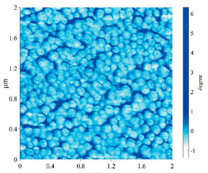
PS-PBMA Copolymer · Phase · 2 × 2 μm
Microphase separation of a block copolymer; phase image clearly resolves the two domains.
Au-Ti Electrode · EFM Lift · 5 × 5 μm
Electrostatic-force imaging of Au-Ti stripe electrodes — the standard EFM teaching sample.
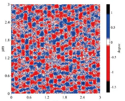
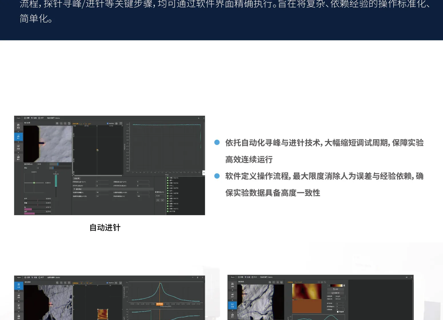
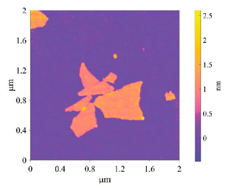
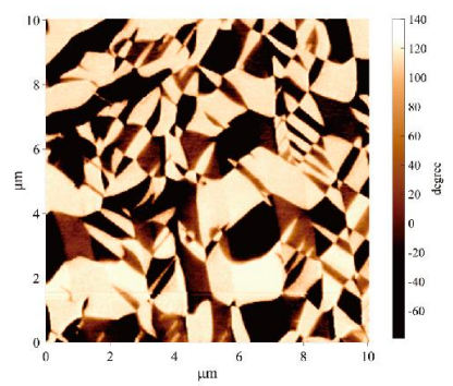
Hard-Disk Track · MFM Lift · 5 × 5 μm
Single-bit magnetic domains from a hard-disk platter, clearly resolved.
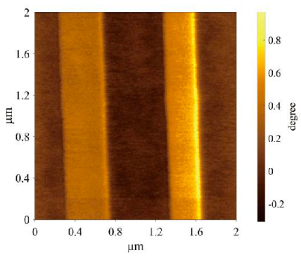
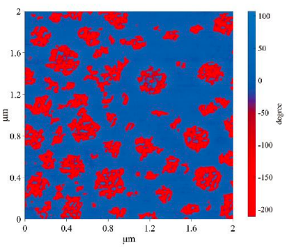
Floppy Tape · MFM Lift · 25 × 25 μm
Classic teaching sample — magnetic-domain stripes illustrate magnetic-recording principles.
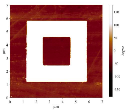
PbTiO₃ · PFM Contact · 3 × 3 μm
Vertical piezoresponse of a ferroelectric film — bright/dark contrast shows domain structure.
PMN-PT · PFM Contact · 5 × 5 μm
Complex domain structure of a relaxor ferroelectric — PFM phase identifies polarization direction.
CuInP₂S₆ · PFM Contact · 3 × 3 μm
In-plane polarization imaging of a 2D ferroelectric — a canonical research-frontier sample.
Real specs. Real data. Real publications.
Publications
AtomControl Lite
Bilingual Real-time Control
EN/CN GUI with live topography preview, auto-approach status, and 4-step automated workflow (Parameters → Approach → Scan → Retract). Switchable anytime — built for bilingual classrooms.
Comprehensive Analysis
Built-in roughness (Ra/Rq/Rz), cross-section profiling, particle analysis, and 3D visualization with publication-quality export and automated PDF reports.
Recipe & Report Management
Save measurement recipes for QA reuse — one-click recall by shop-floor technicians. PDF reports with topography + parameter tables + section data.
Common Questions
Manufactured by Truth Instruments — founded in Qingdao in 2019 with R&D centers in Beijing and Hangzhou. A national-level "Specialized & Sophisticated 'Little Giant'" enterprise; 51% of staff in R&D, holding 70 patents and 31 software copyrights. Deployed across 49+ research institutions including Tsinghua, Peking University, Fudan, Zhejiang, USTC, HIT, CAS Institute of Physics, Westlake University — and industrial customers SMIC, Western Digital, GoerTek, BGI.
Related Products
Ready to Bring AFM into Your Teaching Lab?
Contact our applications team for pricing, lead times, and a live demo.