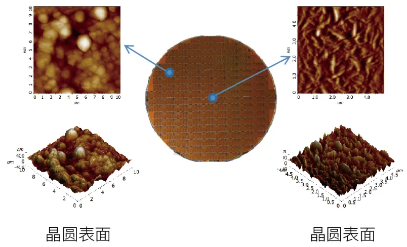
 Wafer roughness · Tapping mode
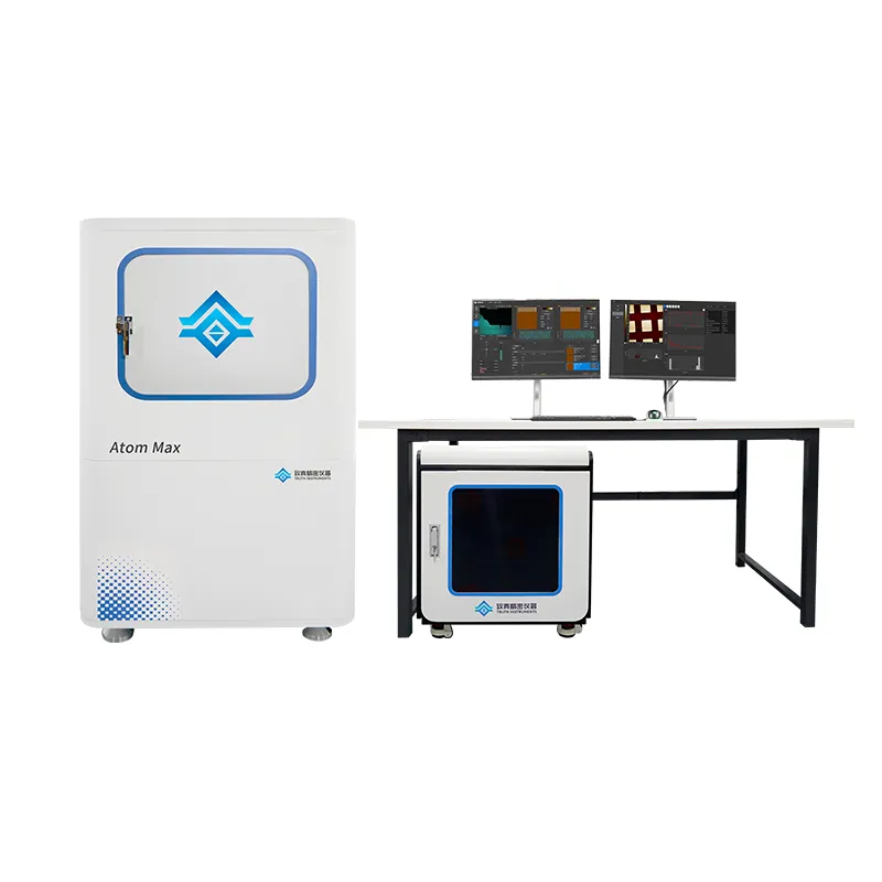
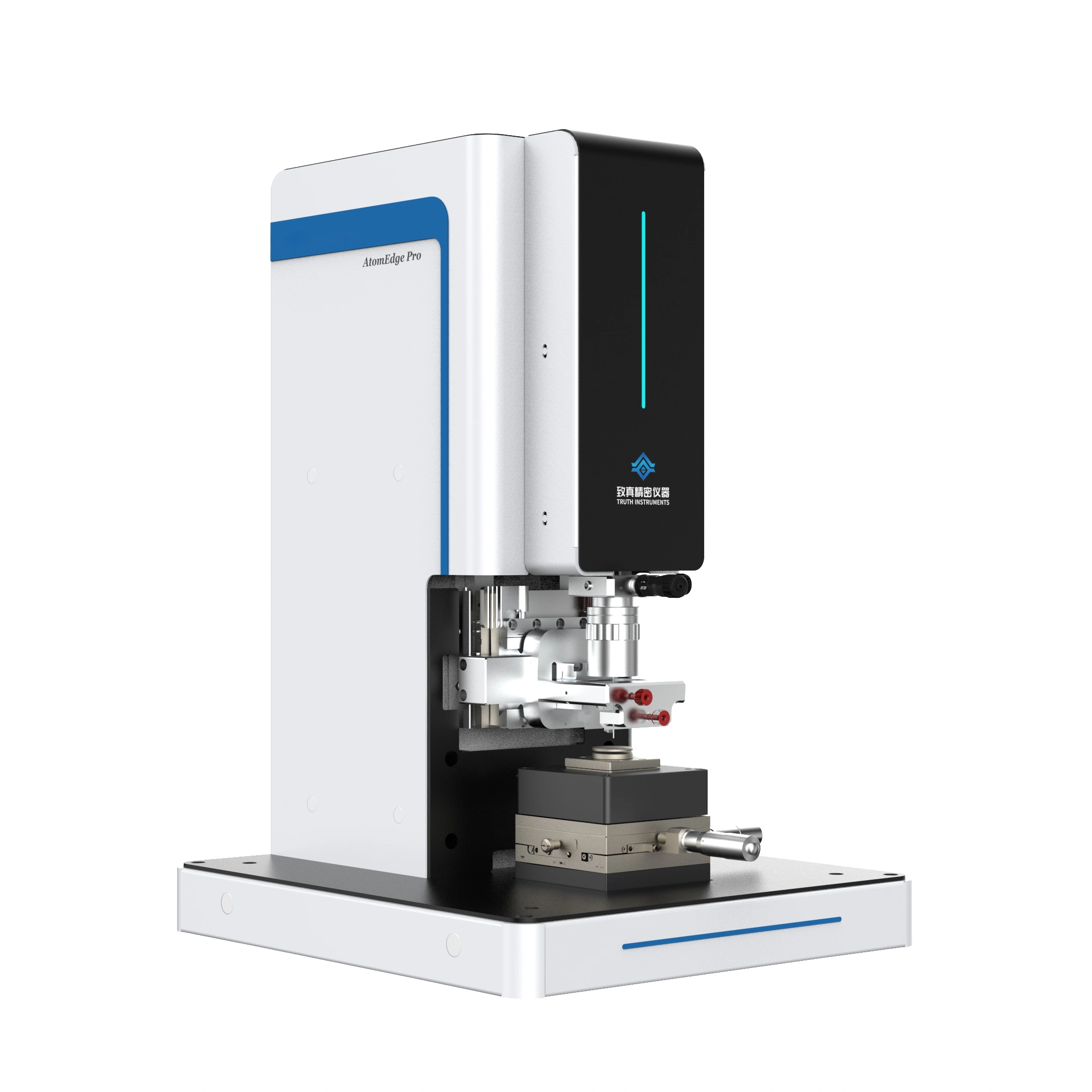
Atom Max
Wafer-Level Multifunctional AFM
An 8-inch wafer-scale AFM platform built for semiconductor, MEMS, and wafer-fab workflows. Orthogonal-decoupled scanner, 0–360° scan angle, and millimeter-class precision stage deliver nanometer metrology anywhere on a full wafer.
A Multifunctional AFM Built for Wafer Metrology
Atom Max brings the full suite of multifunctional AFM modes (EFM / KPFM / PFM / MFM) onto an 8-inch wafer platform, with backward compatibility for 6″, 4″, and piece samples. A 200 × 200 mm stage delivers 1 μm positioning precision — any location on a full wafer can be reached with a single click.
For semiconductor process monitoring, MEMS characterization, and functional-materials R&D where consistency and repeatability are non-negotiable, Atom Max replaces manual stage alignment on conventional benchtop AFMs.
Wafer-Scale Stage
Native 8-inch support; 6″ / 4″ and piece samples without hardware swap.
High-Precision Stage
1 μm positioning precision across 200×200 mm — one-click site recall.
0-360° Scan Angle
Any scan direction — match anisotropic structures or die routing.
Integrated Automation
Auto wafer align / laser find / tip approach / scan — no operator intervention.
Specifications & Technology
| Scan Range (XYZ) | 100 × 100 × 10 μm |
| Scan Angle | 0 – 360° |
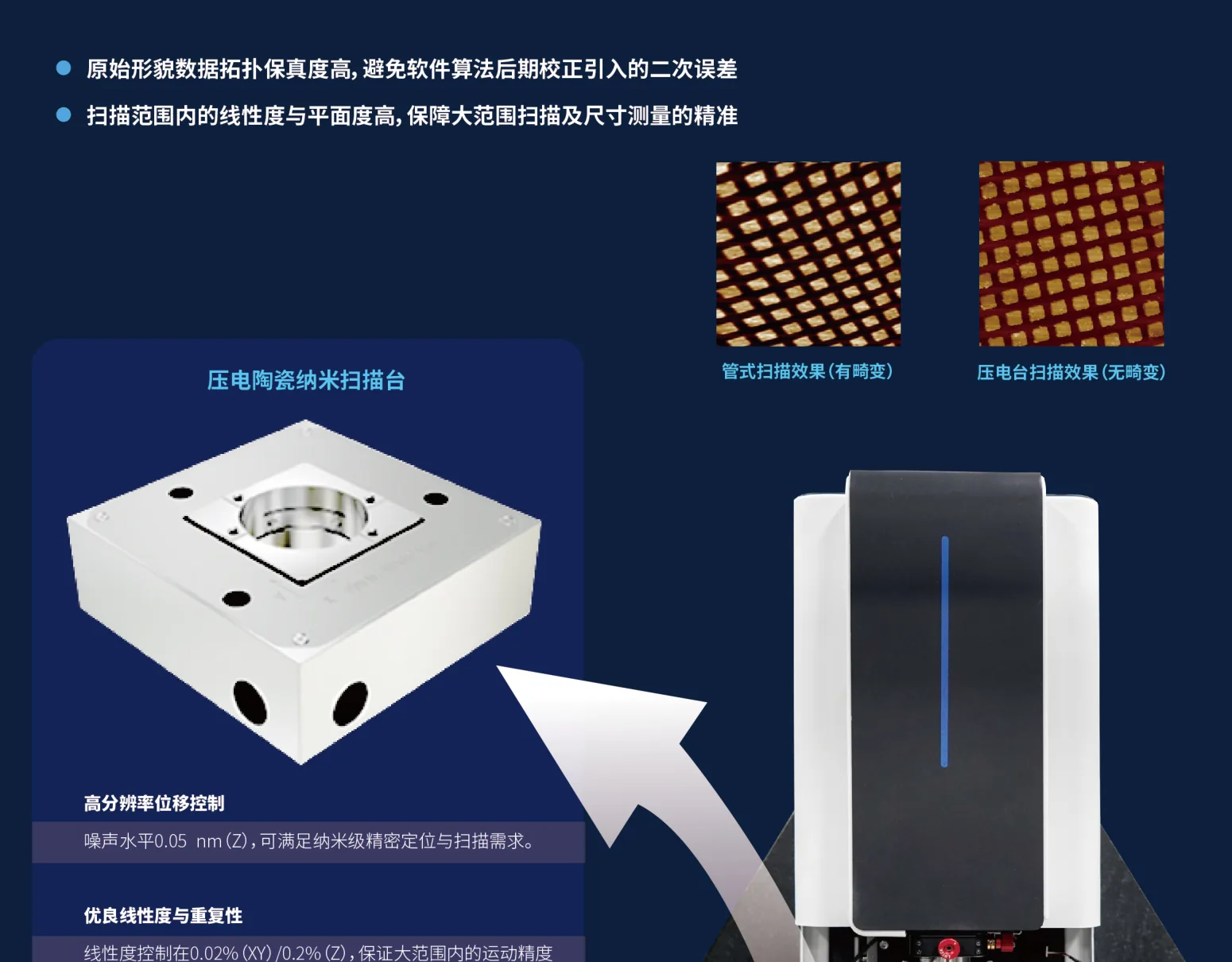
| Z Linearity | 0.2% |
| Z Noise Floor | 0.05 nm |
| Pixel Resolution | 32×32 – 4096×4096 |
| Max Sample | 8-inch wafer (backward-compatible 6″/4″/piece) |
| XY Travel | 200 × 200 mm |
| XY Precision | 1 μm |
| Auto Wafer Align | Supported (vision + coordinates) |
| Standard | Contact / Tapping / Phase / Lift |
| Electrical | EFM / KPFM (lift mode, phase-locked) |
| Magnetic | MFM (lift mode) |
| Piezoelectric | PFM (contact) |
| Optional | C-AFM / SCM |
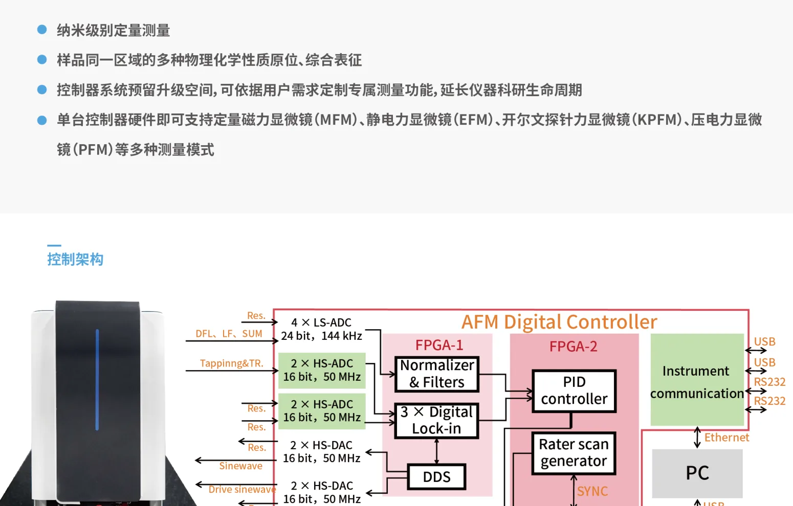
| Architecture | Dual-FPGA parallel |
| Feedback Loop | up to 100 kHz |
| Lock-in Amps | 2 built-in, >1 MHz BW |
| Sync Channels | Up to 12 synchronous |
| Control Software | AtomControl (EN/CN bilingual GUI) |
| Analysis Suite | Roughness / Section / Particles / PSD / 3D |
| AI Assistant | Truth-Seeker (literature / plan / report) |
Wafer-Scale Sample Stage
Native 8-inch wafer handling with backward compatibility for 6″ / 4″ and piece samples — no chuck swap required. The 200 × 200 mm stage delivers 1 μm precision, so moving between sites across a full wafer happens in one operation.
For fab lines and MEMS labs, this closes the loop between process monitoring, defect re-inspection, and batch-consistency analysis on a single tool — with no expensive dicing step in between.
Dual-FPGA Digital Controller
A dual-FPGA hardware-parallel architecture runs three independent feedback loops at up to 100 kHz — 3–10× faster than legacy DSP systems. Two built-in >1 MHz lock-in amplifiers deliver zero-latency synchronous demodulation for EFM / KPFM / PFM — no external lock-in needed.
A single scan captures up to 12 channels simultaneously — topography, phase, amplitude, lateral force, surface potential — all in one pass, with zero inter-channel phase drift.
0-360° Arbitrary-Angle Scanning
Scan direction is freely selectable from 0 – 360° in software. For die routing, anisotropic films, and gradient structures, you can actively choose the optimal angle for highest image SNR.
At wafer scale, this means scanning along a specific device axis to avoid artifacts introduced by the default 0°/90° scan directions.
Integrated Automated Workflow
From wafer load onward: auto wafer align → auto laser find-peak → auto PSD align → auto tip approach → auto scan → auto retract. One-click end-to-end — removes operator variability, critical for multi-user facilities and high-throughput metrology.
Scan tasks can be queued to define many measurement sites across a wafer; the tool runs them sequentially and unattended.
Why Fabs and MEMS Labs Choose Atom Max
From travel range and precision to automation — every parameter is defined for wafer-scale measurement.
Native Wafer Compatibility
8-inch wafers without dicing; backward compatibility down to 6″/4″/piece — one tool from R&D through pilot production.
Millimeter-Range Precision
1 μm positioning over 200 × 200 mm — one-click recall of any site. No coordinate rebuilding between re-measurements.
Z Noise Floor
0.05 nm vertical noise meets the tightest wafer-roughness specs — replaces white-light interferometers for trench depth and CMP roughness.
Any-Angle Scanning
Scan direction chosen in software to avoid axis-aligned artifacts and capture the true structure along any device axis.
Multi-Mode Integration
Topography / EFM / KPFM / PFM / MFM / Phase / C-AFM — switch in software, multi-physics characterization in a single mount.
End-to-End Automation
Auto wafer align, find-peak, approach, scan — eliminates operator variability. Ideal for shared facilities.
Real Scans from the Field
Real data from Truth Instruments' Atom Max wafer-level AFM across semiconductor, photovoltaics, magnetic, and piezoelectric materials.
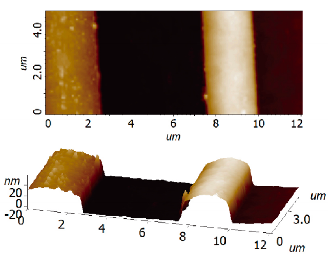
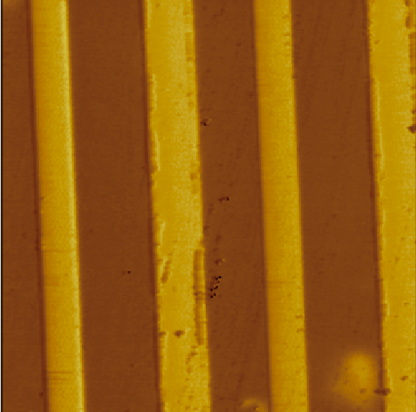
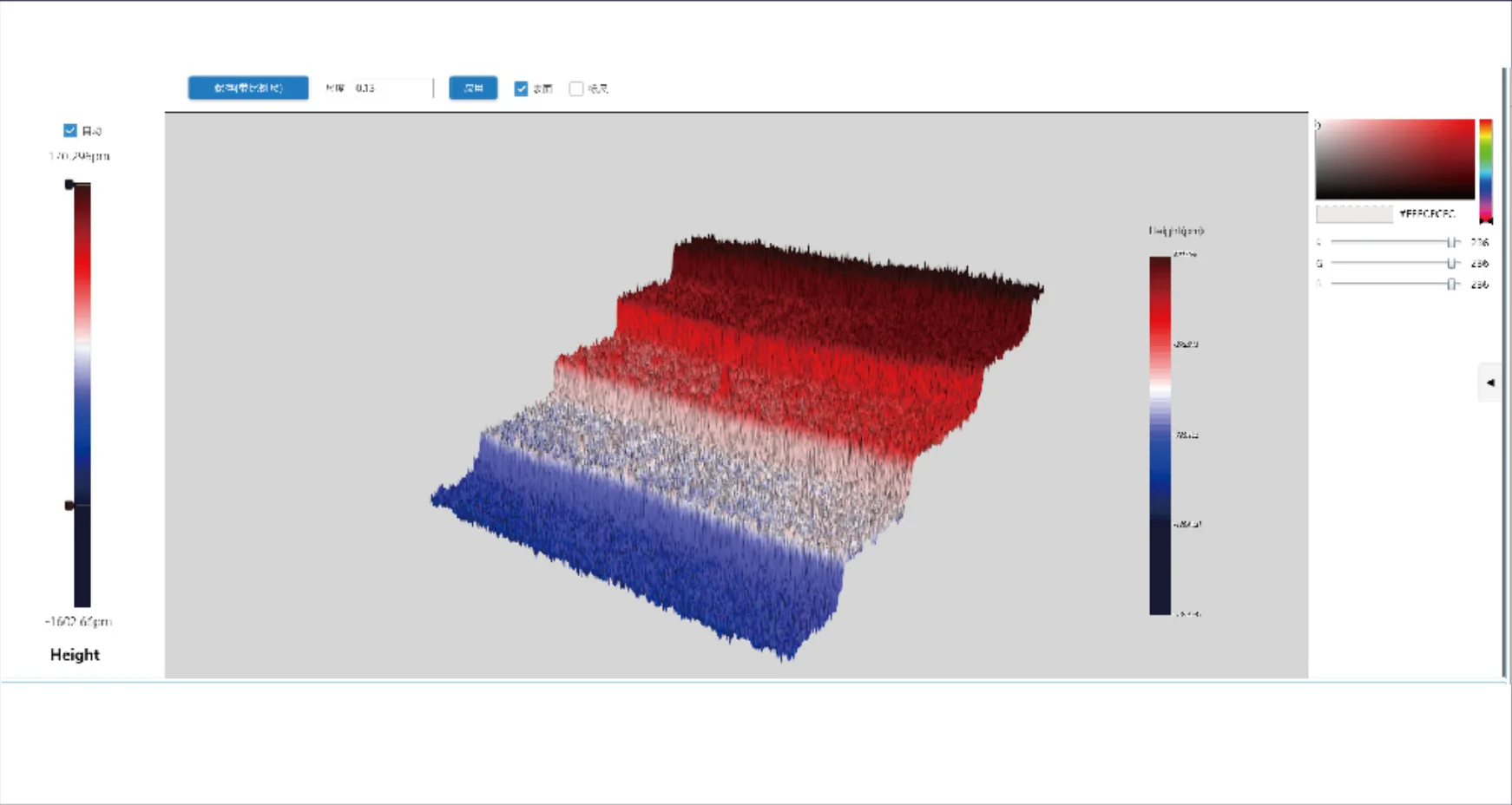
Wafer Trench Depth · Tapping Mode
Deep-trench structures on an 8-inch wafer; 0.05 nm Z noise enables sub-nanometer depth measurement — a direct replacement for optical interferometers.
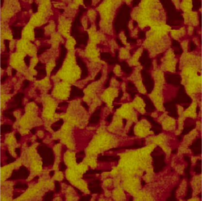
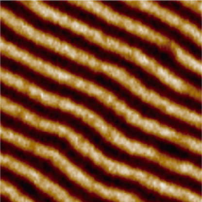
Wafer Roughness · Tapping Mode
Post-CMP silicon wafer surface roughness — Ra / Rq / Rz reported simultaneously.
CZTSSe Film · KPFM Lift Mode
Surface potential distribution of thin-film solar absorber; resolves grain-boundary potential differences.

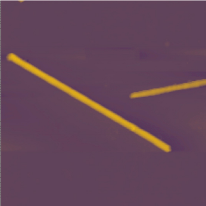
Au-Ti Electrode · KPFM Lift Mode
Surface-potential imaging on Au-Ti stripe electrodes; resolves work-function contrast vs. substrate.
Au-Ti Electrode · EFM Lift Mode
Electrostatic-force imaging of the same electrode sample — complementary to KPFM.
Fe-Ni Magnetic Domains · MFM Lift Mode
Soft-magnetic-film domain structure; two-pass imaging cleanly separates topography and magnetic signal.
PbTiO₃ · PFM Contact Mode
Vertical piezo-response amplitude imaging — accurate ferroelectric domain structure.
SiC Whisker · Tapping Mode
Third-generation semiconductor topography — resolves single-whisker surface features.
Wafer-grade specs. Production-grade data.
Publications
AtomControl
Bilingual Real-time Control
EN/CN GUI with wafer map display, live topography preview, auto-approach status, and queue-based multi-site scan management.
Publication-Grade Analysis
Ra/Rq/Rz/Sa/Sq roughness (ISO/ASME), section profiling, particle count, PSD, and 3D visualization with publication-quality export.
Truth-Seeker AI
Proprietary AI for literature search, experiment planning, automated image analysis, and structured report generation.
Common Questions
Manufactured by Truth Instruments — founded in Qingdao in 2019 with R&D centers in Beijing and Hangzhou. A national-level "Specialized & Sophisticated 'Little Giant'" enterprise; 51% of staff in R&D, holding 70 patents and 31 software copyrights. Deployed across 49+ research institutions including Tsinghua, Peking University, Fudan, Zhejiang, USTC, HIT, CAS Institute of Physics, Westlake University — and industrial customers SMIC, Western Digital, GoerTek, BGI.
Related Products
Ready for Wafer-Level AFM Metrology?
Contact our applications team for pricing, lead times, and a live demo.