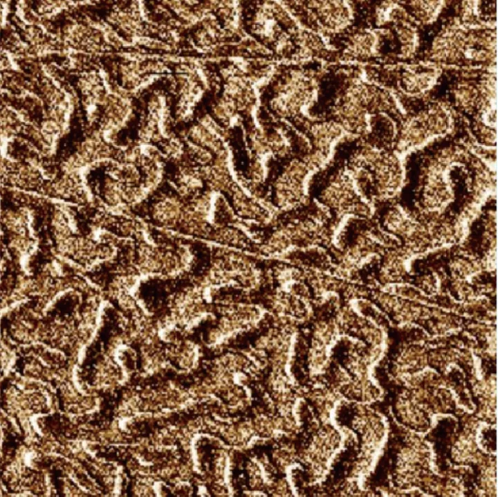
 Grating topography · Tapping mode
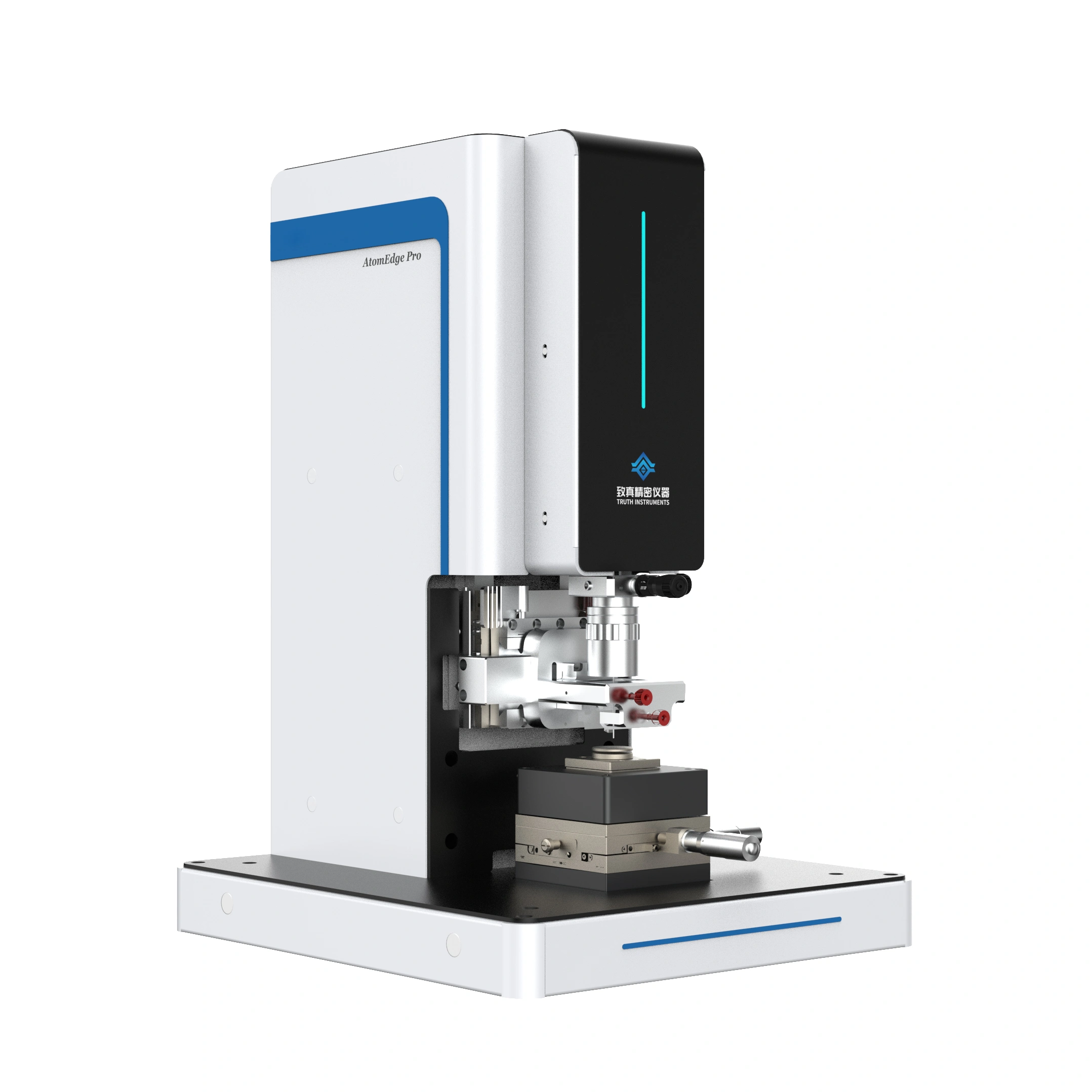
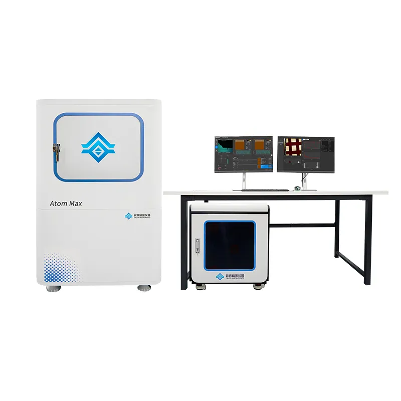
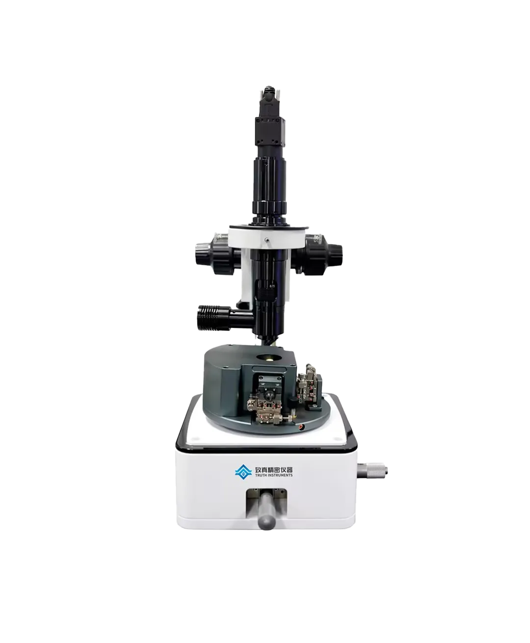
AtomEdge Pro
Multi-functional Atomic Force Microscope
Sub-angstrom resolution AFM with AI-powered analysis. Engineered for nanoscale surface characterization, multi-modal imaging, and intelligent automation.
The Researcher's Multi-Mode Workhorse
The AtomEdge Pro combines sub-angstrom resolution, a fully decoupled orthogonal scanner, and a dual-FPGA controller — covering 7+ imaging modes from topography to KPFM, MFM, PFM, and in-situ liquid-cell measurements without hardware changes.
Backed by 70 patents and deployed in 49+ Chinese research institutes. Engineered for researchers who need reliable, artifact-free quantitative data.
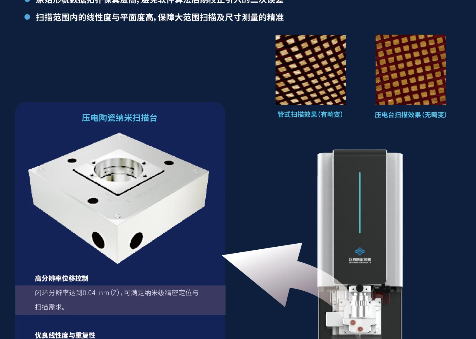
Orthogonal Decoupled Scanner
Three-axis capacitive closed-loop with 0.02% XY linearity. Artifact-free across the full 100 μm range.
SLD Laser Detection
<50 fm/√Hz noise floor. Resolves 0.39 nm SrTiO₃ atomic steps that laser-diode heads cannot.
Dual-FPGA @ 100 KHz
3-loop hardware feedback with 2 integrated lock-in amplifiers. 12 synchronized channels in one pass.
Specifications & Technology
| Scan Range (XYZ) | 100 μm × 100 μm × 10 μm |
| Z Closed-loop Resolution | 0.04 nm |
| XY / Z Linearity | 0.02% / 0.08% |
| Vertical Resolution | <0.1 nm (RMS < 40 pm) |
| Noise Floor | <50 fm/√Hz (SLD) |
| Scan Rate | 0.1 – 30 Hz |
| Image Resolution | 32×32 – 4096×4096 px |
| Scanner Type | 3-axis orthogonal decoupled, capacitive closed-loop |
| Standard | Contact, Tapping, Phase, Lift, Multi-directional |
| Electrical | EFM, KPFM, PFM; Optional: C-AFM, SCM |
| Magnetic | MFM (two-pass lift) |
| In-situ | Liquid cell, light illumination, electrochemical, thermal |
| Laser Source | Superluminescent Diode (SLD) S650.7.3, low coherence |
| Camera | Color CMOS, 5 MP, real-time video |
| Field of View | 1680 × 1410 μm |
| Objective | 10× (optional 20×, 50×) |
| Optical Resolution | 1 μm |
| Motorized Focus | Yes, with auto-focus |
| Architecture | Dual high-speed FPGA |
| Converters | ≥8 DAC (XYZ 20-bit + 16-bit user + 20-bit bias), ≥10 ADC (4 ch > 50 MHz) |
| Feedback Loops | 3 independent, parallel |
| Lock-in Amplifiers | 2 integrated, > 1 MHz bandwidth, 0.1 Hz resolution |
| Data Channels | 12 simultaneous, time-synchronized |
| Feedback Rate | Up to 100 KHz |
| Sample Stage | Up to φ25 mm; motorized XY ±12.5 mm |
| Vibration Isolation | Marble air table + acoustic enclosure (opt. active) |
| Tip Protection | Automated safe approach with force limit |
| Thermal Drift | <1 nm/min (after 30-min warmup) |
| Glove-Box | Yes (optional compact head) |
| Environment | Lab, cleanroom, glove-box; optional enclosure |
| AI Module | Truth-Seeker AI — literature search, experiment planning, auto analysis, report generation |
| Control Software | Bilingual (EN/CN) GUI, real-time monitoring, 4-step workflow (Param → Approach → Scan → Retract) |
| Analysis Suite | Roughness, particle/pore, cross-section, PSD, 3D visualization, multi-format export |
Orthogonal Decoupled Piezo Scanner
Three-axis orthogonal decoupled design with independent capacitive sensors per axis. Achieves 0.02% XY linearity and 0.08% Z linearity across the full 100 μm × 100 μm × 10 μm range. Reduces scanner bow to below 0.2 nm — one to two orders of magnitude better than tube scanners, which typically introduce 5–20 nm of background curvature.
For researchers, this means reliable step-height metrology, faithful thin-film roughness, and any measurement requiring accurate height data — without post-processing background subtraction.
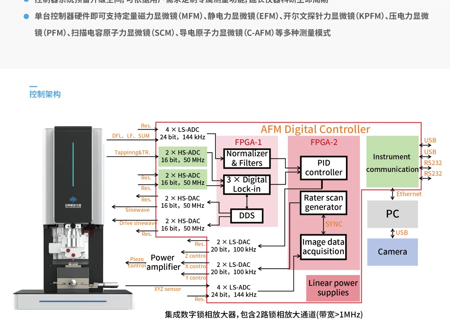
Dual-FPGA Digital Controller
Hardware-level parallel processing for 3 independent feedback loops at up to 100 KHz — 3–10× faster than DSP-based systems. Two on-board lock-in amplifiers (>1 MHz bandwidth, 0.1 Hz resolution) provide zero-latency synchronous demodulation for EFM, KPFM, PFM, and other AC modes. No external lock-ins, no cabling delay.
Supports 12-channel time-synchronized data acquisition in a single scan pass — topography, phase, amplitude, lateral force, CPD, and up to 7 user-configurable auxiliaries.
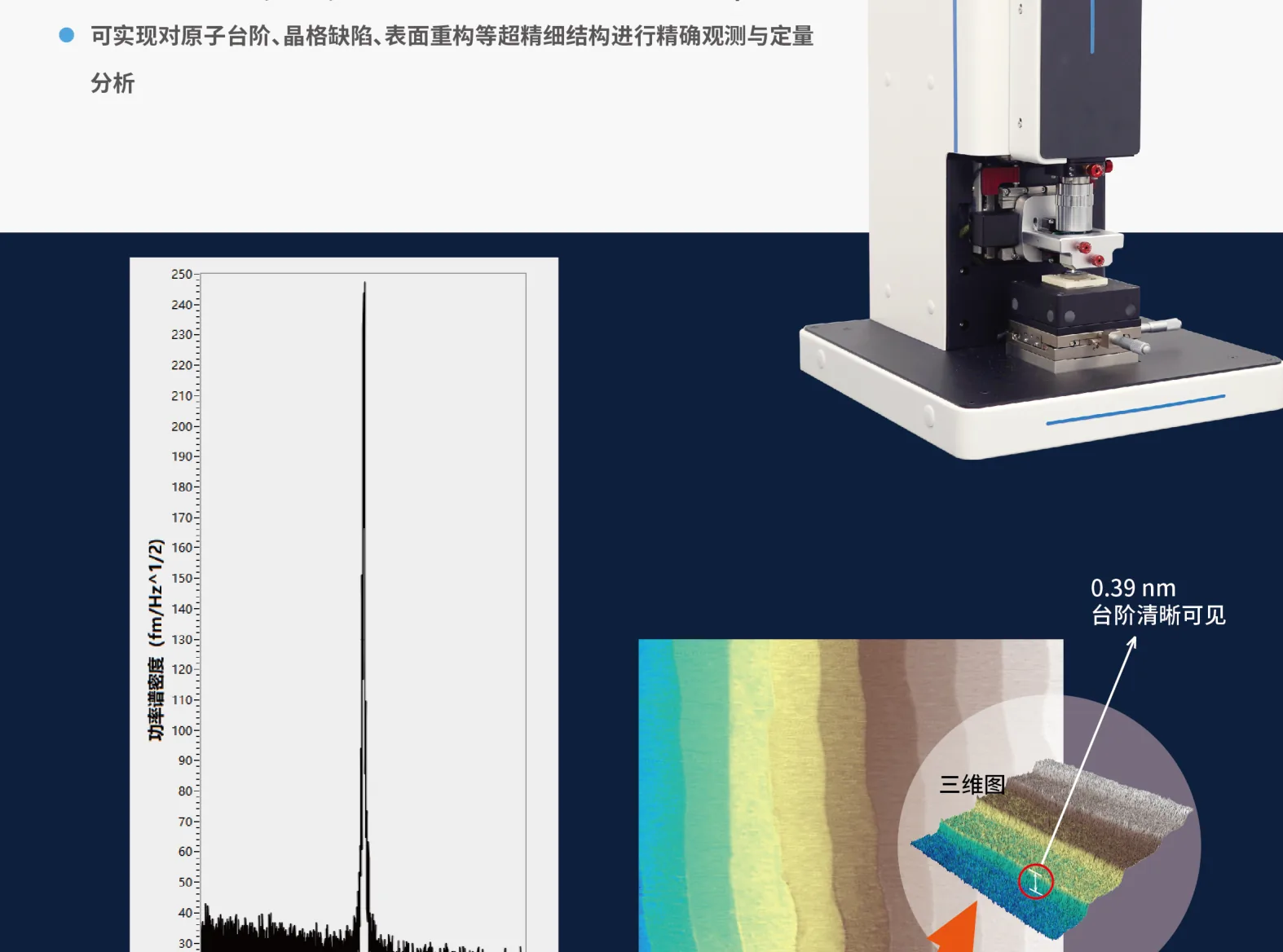
Superluminescent Diode (SLD) Laser
Broadband, low-coherence SLD source (coherence length <30 μm) virtually eliminates optical interference noise between the cantilever and nearby reflective surfaces. Drives the noise floor below 50 fm/√Hz and delivers vertical resolution better than 0.1 nm (RMS <40 pm) — less than half the diameter of a water molecule.
In practice: resolves 0.39 nm SrTiO₃ atomic steps, detects sub-monolayer film nucleation, and enables piconewton-level biological force spectroscopy that conventional laser-diode AFMs cannot achieve.
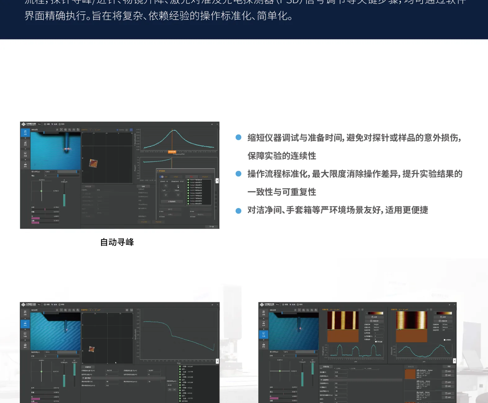
Integrated Automation & Glove-Box Ready
Fully automated 4-step workflow — Parameters → Approach → Scan → Retract — with one-click auto-find-peak, auto-approach, auto laser alignment, and PSD optimization. Reduces operator dependency and learning curve, delivering repeatable results across operators.
Compact head option integrates directly into glove-boxes and cleanrooms, with controller/computer outside the chamber via feedthrough. Essential for air-sensitive samples, inert-atmosphere studies, and multi-user research facilities.
Six engineering choices that change what you can measure
Every subsystem is specified to push noise floor, precision, and throughput — the thresholds that skyrmion imaging, quantitative KPFM, and nano-mechanics actually demand.
SLD Laser Displacement Sensor
Sub-angstrom noise floor enables reliable quantification of topological Hall signatures and sub-nanometer magnetic textures that laser-diode heads cannot resolve.
Orthogonal Decoupled Flexure Scanner
XY linearity of 0.02% with capacitive closed-loop feedback removes scanner bow and axis cross-coupling — faithful quantitative mapping across the full 100 μm range.
Picometer-Class Z Positioning
Closed-loop resolution holds the tip on a single lattice site through hours of scanning — the prerequisite for atomic-step imaging and repeatable force-curve arrays.
Complete Multi-Mode Suite
Contact / Tapping / KPFM / MFM / PFM / EFM / C-AFM / SCM — software-switchable on one platform. One workflow, one control loop, no probe-holder swaps.
Liquid, Light, Electrical, Thermal
Engineered accessory line supports photocatalysis, electrochemistry, and variable-temperature studies — published in JCIS and Int. J. Hydrogen Energy.
Institutes Served
Deployed across top Chinese universities and national labs including Peking Univ., Zhejiang Univ., Fudan, USTC, HIT, and CAS Institute of Physics. Referenced in peer-reviewed publications on magnetism, catalysis, and semiconductor materials.
Truth-Seeker AI — your on-instrument research assistant
A self-developed AI model that turns the AFM from a data-acquisition device into an intelligent research platform. Truth-Seeker handles the tedious research-workflow tasks — so your time goes to science, not SOPs.
Literature Retrieval
Surfaces and summarizes the latest papers on your sample and measurement mode in seconds.
Experiment Design
Recommends scan parameters, probe type, and protocol from a natural-language description.
Standardized Guidance
Step-by-step operation that lowers the learning barrier and keeps results consistent.
Automated Reporting
Processes acquired data into structured reports with figures and publication-ready formatting.
Over the past five years, PFM-based studies on 2D ferroelectrics have converged on three hotspots:
① Polar skyrmion bubbles — CuInP₂Se₆, Nat. Commun. (2025) · DOI:10.1038/s41467-025-57714-9
② Two-dimensional piezoelectric diodes — α-In₂Se₃, Nanoscale (2018)
③ Ultrathin HfO₂ ferroelectricity — Nature 580, 478 (2020)
Recommended workflow: (1) probe install — tapping probe; (2) sample mount — magnetic puck; (3) laser alignment — use auto-align; (4) scan params — 5×5 μm, 256×256 px, 1 Hz; (5) run auto-approach; (6) begin scan.
Real Scan Data
Published gallery from Truth Instruments customers — materials science, magnetics, ferroelectrics, electrochemistry, and life sciences.
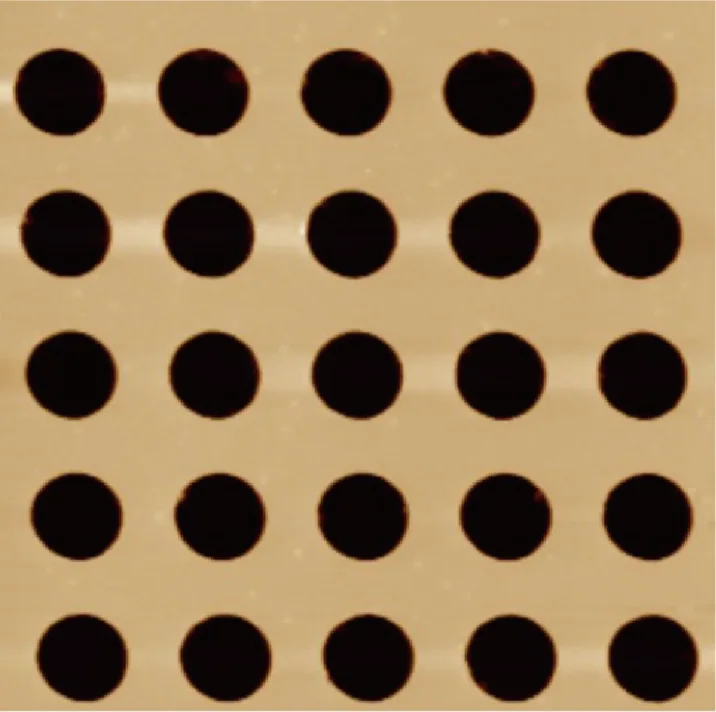
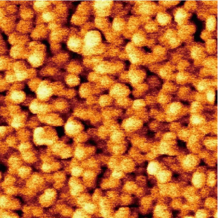
Grid Reference Sample · Tapping Mode · 25 × 25 μm
Periodic calibration standard imaged at 25 × 25 μm — demonstrates scanner linearity and closed-loop accuracy.
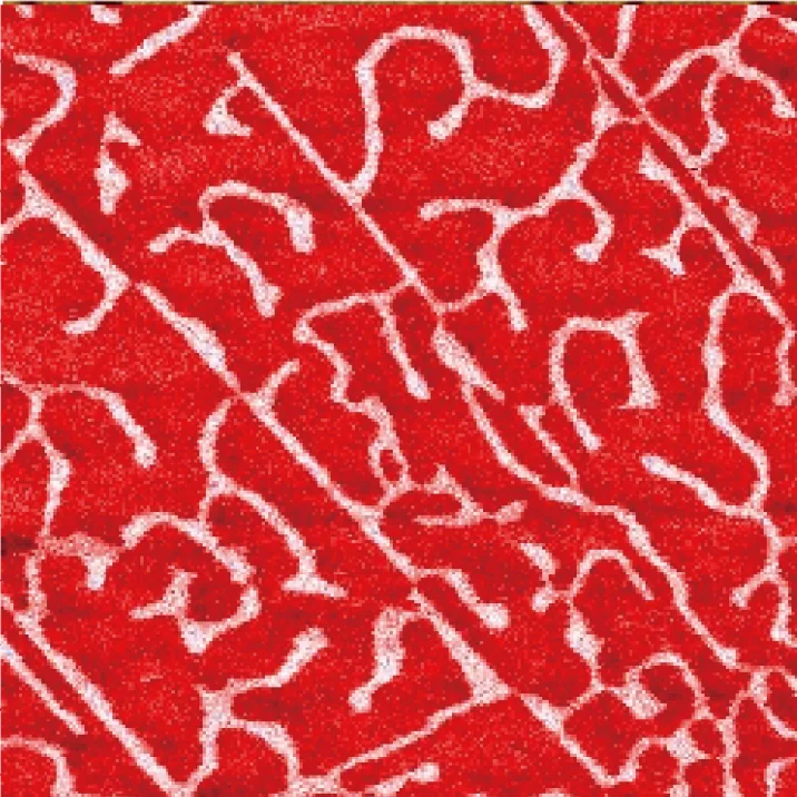
PbTiO₃–PMN · PFM Mode · 10 × 10 μm
Ferroelectric domain switching and piezoresponse imaging on lead titanate–lead magnesium niobate ceramics.
Bismuth Vanadate · EFM Mode · 5 × 5 μm
Electrostatic force microscopy on photoactive BiVO₄ thin film — resolves local charge trap distribution.
Bismuth Vanadate · KPFM Mode · 5 × 5 μm
Kelvin probe force microscopy on the same BiVO₄ film — contact potential mapping of grain-to-grain variation.
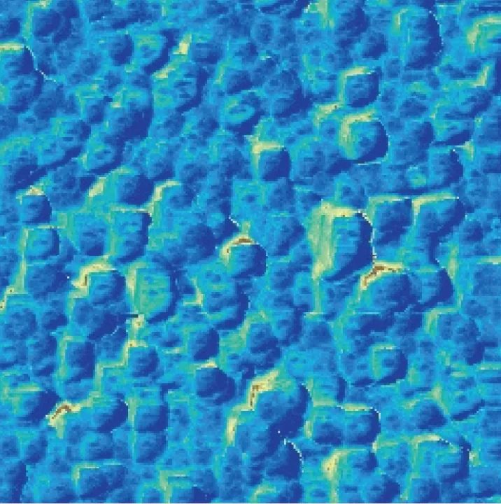
Co/Fe/B Thin Film · MFM Mode · 25 × 25 μm
Magnetic domain structure in Co/Fe/B multilayer — two-pass lift mode reveals domain walls and stripe patterns.
Co/Pt Thin Film · MFM Mode · 30 × 30 μm
Perpendicular magnetic anisotropy domain structure in Co/Pt multilayer — foundation for skyrmion research.
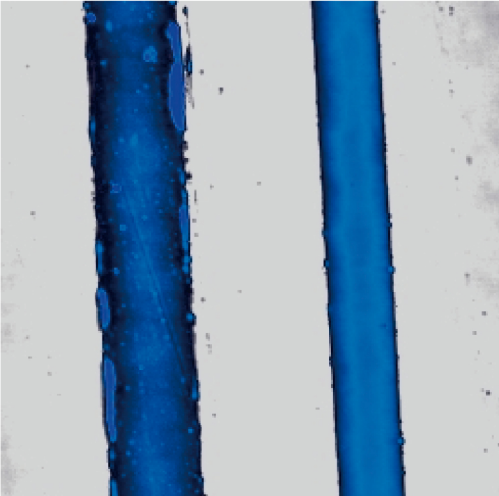
Au-Ti Strip Electrode · Tapping Mode · 18 × 18 μm
Surface topography of gold-titanium strip electrode — used in semiconductor and MEMS device characterization.
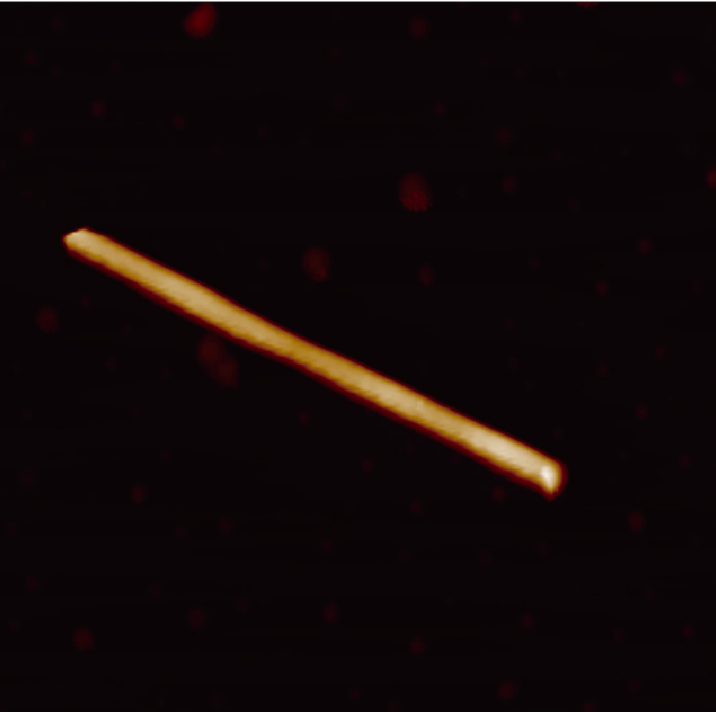
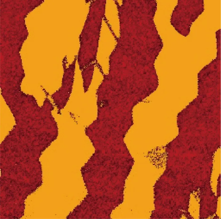
Al₂O₃ Whisker · Tapping Mode · 15 × 15 μm
Single alumina whisker imaged against a flat substrate — demonstrates low-noise imaging of isolated nanowire features.
Specifications you can cite. Research you can verify.
Publications
Intelligent AFM Software
Real-time Control Software
Bilingual EN/CN GUI with live topography preview, auto-approach status, intelligent parameter optimization, and 4-step automated workflow (Parameters → Approach → Scan → Retract).
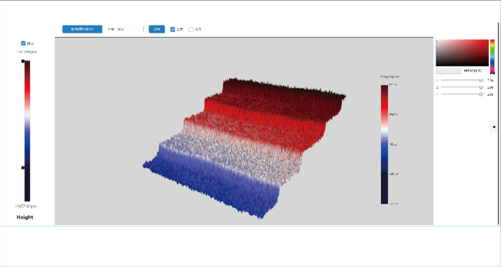
Comprehensive Analysis Suite
Built-in roughness (Ra/Rq/Rz), particle/pore analysis, cross-section profiling, power spectral density, and 3D visualization with publication-quality export.
Truth-Seeker AI
Proprietary AI for literature search, experiment planning, automated image analysis, and structured report generation — see the AI section above for details.
Common Questions
Manufactured by Truth Instruments (致真精密仪器) — a National "Little Giant" enterprise founded in 2019, headquartered in Qingdao with R&D centers in Beijing and Hangzhou. 51% of staff are dedicated to R&D; the company holds 70 patents and 31 software copyrights across its AFM product line. Their instruments are deployed at 49+ leading institutions including Tsinghua, Peking University, Fudan, Zhejiang University, USTC, HIT, CAS Institute of Physics, and Westlake University — as well as industry leaders like SMIC, Western Digital, Goertek, and BGI.
Related Products
Ready to Explore Sub-Angstrom Resolution?
Contact our applications team for pricing, lead times, and a live demo.